Tento materiál pochádza z časopisu ANTIC a nie každý má možnosť sa k týmto veciam dostať tak zase niečo na tému software a a hardware. Články boli uverejnené v nasledovných číslach:
Antic Vol. 3 No. 9 - January 1985
Antic Vol. 3 No. 10 - February 1985
Antic Vol. 3 No. 11 - March 1985
Antic Vol. 3 No. 12 - April 1985
____________________________________________________________
1
THE PARALLEL BUS REVEALED
100,000 bytes per-second
Part one of a four-part series
by EARL RICE
Until now, the Parallel Bus Interface has been one of the big mysteries of Atari XL computers. This important Antic series-by one of Atari's former top technical executives-will at last provide all the information necessary for tapping the power of this 100,000 byte per second connection.
If you own an Atari 600XL or 800XL, you've probably noticed a little plastic cover on the back. Above that cover are the Words "PARALLEL BUS." Until now, this port has only been used for memory expansion cartridges.
Then last June at the Consumer Electronics Show, the Atari company finally released full specifications for the Parallel Bus Interface (PBI). This series of articles is based on that information.
In the next few issues of Antic, we'll explain how the parallel bus works and how you can use it with your own projects.
IMPORTANCE OF THE PBI
The parallel bus interface runs at the same speed as the 6502 microprocessor-and it can transfer information more than 40 times faster than the serial connector.
The serial connector can transfer no more than 2400 bytes per second. The parallel bus can easily transfer 100,000 bytes or more per second, depending on software execution speed. This speed allows you to design controllers for hard disks and other high-speed devices.
WHAT THE PBI IS
Basically, the parallel bus connector is an extension of the 6502 data, address, and control signals. These signals aren't buffered, and can drive only a very limited electrical load. Unmodified, there isn't very much you can do with the PBI. When used with appropriate software and hardware, however, the PBI becomes an extremely powerful extension of your computer.
Fortunately, the PBI's design is easy to understand. Additionally, most of the software you'll need is already in the Operating System. This code, called the Generic Parallel Device Handler, resides at location 58511 ($E48F), just waiting to talk to your high-speed devices. All you have to do is write the low-level hardware driver software and combine it with your hardware.
But first you need to see how the PBI works.
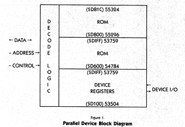
A parallel device (Figure 1) is essentially a circuit board containing five key elements:
- A ROM chip containing both the low-level driver software and a Device Handler Table.
- Any RAM required for on-board buffers.
- Some address-decoding logic.
- A hardware-select register.
- The functional circuitry itself. (Perhaps an I/O device such as a universal asynchronous receiver/ transmitter (UART) to drive a modem, or a parallel interface adapter (PIA) to drive a printer.)
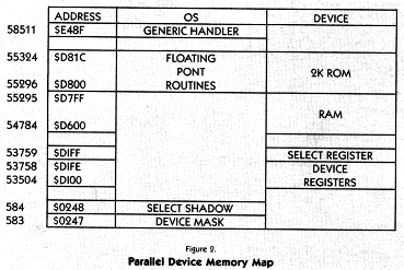
All device registers, ROM, and RAM are mapped into your computer's memory space as shown in the simplified memory map (Figure 2).
The PBI's ROM space is mapped into the same area as the OS conversion routines from ASCII to Floating Point. The computer's memory management IC switches out the OS ROM when an external device is selected, and switches back in when it's done. The catch is that your external device can't use the floating point software in the OS. it also can't use any function of the OS or application software (like BASIC) that uses floating point routines.
Since most external devices are essentially I/O peripherals, these restrictions should not create many programming problems.
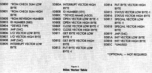
The first 26 bytes of ROM contain a data table (Figure 3). This is a handler table which has the same format as the other OS vector tables. Note that some of the data is optional. The required data consists of ID bytes used by the Generic Handler to validate the presence of a parallel device, and JUMP vectors to device functions.
During a coldstart, just before attempting to initialize a cartridge, the OS will poll for parallel devices. If the ID bytes are correct, the OS will execute the JMP to the INIT routine at 55321 ($D819) through 55323 ($D81B). This routine must put the address of the Generic Handler (58511, or $E48F) into the OS handler table (HATABS) along with the device name (T:, for example).
That done, your routine sets its select bit in the Device Mask, performs any device-specific initializations and ends with an RTS instruction.
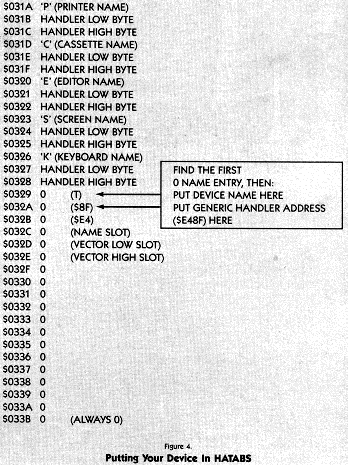
That's really all it takes to let the OS "talk" to your device. Of course, there are the low-level device drivers to consider, but we'll examine them in a later article. For now, remember that the OS simply needs to know that your device exists (have its bit set in the Device Mask) and to have the Generic Handler's address in HATABS (Figure 4).
The OS can handle up to eight devices on the PBI. The OS selects a device by setting the appropriate bit in the Hardware Select register, located at 53759 ($DIFF). BIT 0 selects DEVICE 0, BIT 1 selects DEVICE 1, and so on.
Just like the other registers in the corn this one has a shadow location. The computer uses shadow registers to update the values in its hardware registers. These values are updated 30 times per second. The Hardware Select register's shadow location is at 583 ($0247).
SELECTING DEVICES
Before selecting a device, the OS looks at the Device Mask (location 583, $0247) to see if such a device really exists. Recall that this was the bit set by the initialization routine.
Parameters are passed between the OS and the device using the A, X and Y registers plus the Page Zero I/O Control Block (IOCB).
The carry flag tells the OS whether or not the device performed its requested function. The device sets the flag when it has performed its function. Otherwise, the carry flag is left RESET (0).
The A register passes a data byte, the X register contains the index to the originating device's IOCB, and the Y register contains a Device Status byte. This is the same as any other Central I/O (CIO) operation.
By the way, this is a good place to mention that Atari's Technical Reference Notes (CO16555 Rev. A) are worth their weight in system errors. The basic operation of CIO, IOCB'S, Device Status codes and the like are all presented concisely. If you are serious about writing professional-level software or designing any kind of hardware for the Atari computer, this manual is a must. As we go along, I'll briefly explain the concepts you need for these articles, but these explanations are not offered as a substitute for the Tech Reference Notes.
SUMMING UP
So far we've learned: The OS contains a Generic Handler for parallel devices. It selects one of up to eight devices through a hardware register and keeps track of it through a shadow register. The parallel device has a ROM containing low-level driver vectors (and, perhaps, the drivers themselves) and an INIT routine. During coldstart, the OS will run the INIT routine and the device will declare its existence by writing its bit into the Device Mask and putting its name, along with the Generic Handler's address into HATABS. In operation, the device and the OS communicate through the 6502's A, X, and Y registers plus the Page Zero IOCB. The parallel device cannot use OS Floating Point routines because the device's ROM is mapped into those same locations.
Not too hard, huh? Next month we'll look at hardware requirements, and after that, we'll work up an example and look at interrupts. In the meantime, try to resist the urge to tear off that little cover. We'll explain how to do it safely in the next Antic.
Earl Rice held a number of high-level technical positions at Atari, including head of users group support. His last post there was project leader of the projected top-of-the-line 1450XL computer.
________________________________________________________________________________
2
the toolbox
PARALLEL BUS REVEALED
100,000 bytes per second
Part II of a four part series
by EARL RICE
For the first time, advanced users of the Atari 800XL and 600XL. learn bow it's possible to connect peripherals to the fast, powerful Parallel Bus Interface. Part 2 of a 4-part series.
Last month we looked at the general operation of the Parallel Bus Interface (PBI) emphasizing software concepts. This month, we'll look at the hardware concepts involved in making an external device work via the parallel bus.
Figure 1 shows the basic requirements for a simple serial I/O function such as an RS-232 board. The serial I/O device can be an integrated circuit that looks like a set of registers to the computer. The decode logic selects the device when the assigned PBI addresses are presented on the address bus.
Beyond that, the computer needs to be able to read and write data to the device and respond to its requests for service. That's what the Read/ Write and Interrupt Request lines are for.
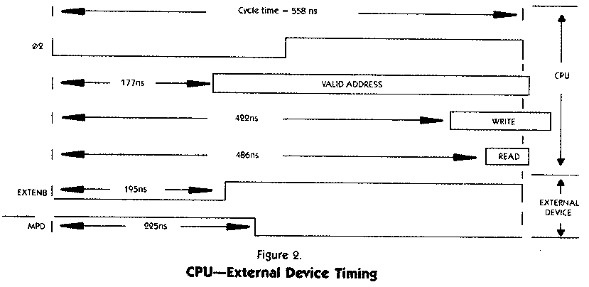
When the computer wants to talk to a parallel bus peripheral, it enables the decode logic with a signal called External Enable. The decode logic decides whether the address on the bus is for the device or for the 2K ROM.
If it's for the ROM, the decode logic returns a Math Pack Disable signal to the computer so that internal ROM won't contend with the 2K ROM for the data bus.
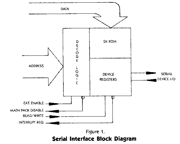
Figure 2 shows the approximate timing of the External Enable (EXTENB) and Math Pack Disable (MPD) signals.
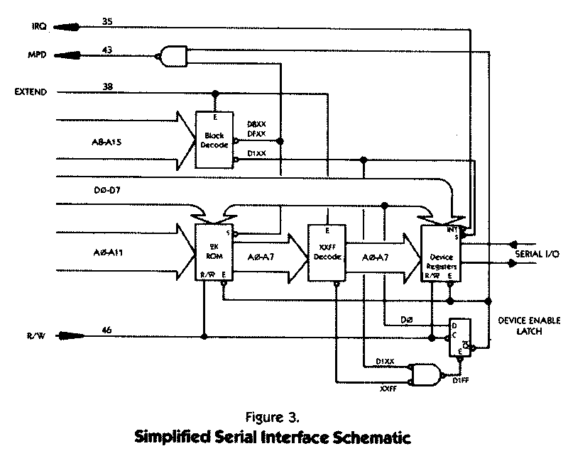
Figure 3 is a more detailed schematic of the hardware example. This is still not the complete design, but it serves to illustrate the concepts some more.
The decode logic does several things:
- Decodes the $D8XX-$DFXX block to enable the 2K ROM.
- Decodes the D1XX block for device registers.
- Decodes the address $XXFF so the computer can select the Device Enable latch at $D1FF. This latch represents the select bit in the Device Select register (DEVSEL).
In Figure 3, the latch is tied to the data 0 line (for device 0). But it could be tied to another line to make the device respond to a different ID number-such as bit 3 for device 3. For simplicity, the latch is a write-only bit. When we expand to a full design, we'll see how to make a readable register. We would need to do that to make the peripheral available to an interrupt service routine.
The Device Enable latch must be set to allow the computer to address the 2K ROM or the device registers. Its output is also gated with the 2K ROM select line to send the MPD signal to the computer. The Device Enable latch is set by writing a I to $D1FF. It is reset by writing a 0 to $D1FF.
SUMMARY
The basic concept isn't hard. The external hardware is enabled by EXTENB. It must decode the 2K ROM space, device registers, and Device Select register. When the 2K ROM is selected, it must return a Math Pack Disable signal to the computer. If the device is interrupt driven, it must supply an interrupt Request(IRQ) to let the computer know it. wants to be serviced. In that event it will also need to supply an IRQ ID number to the computer.
Simple? Sure is ... At least at the conceptual level. It gets a little more involved when we design the decoder and have to deal with timing. We'll do that next month. In the meantime, here's some additional information to help you understand the diagrams:
READING THE DIAGRAMS
Some of the signal names in Figure 3, have a bar over them. That means the signal's active state is low (binary 0). The little circles on the signal lines next to some of the symbols mean the same thing. A dot at the intersection of two lines means they are connected. If they cross without a dot, they aren't connected. The wide arrows indicate multiple signal lines. The numbers inside the arrows tell you which signals are involved. For example, the arrow with A0-A11 means the address fines for address bit 0 through address bit 11 all go to the 2K ROM. Only address bits A0-A7 go to the $XXFF decoder and the device registers, however.
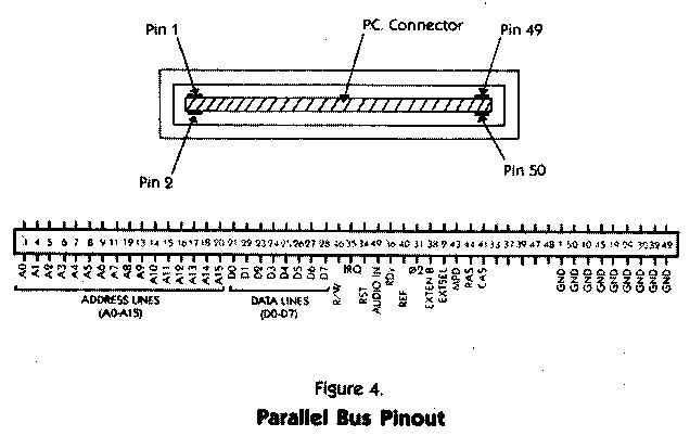
Figure 4 shows the pin numbers for the PBI signals. It also shows how the pins are numbered on the printed circuit connector at the back of your 800XL computer. Imagine you are looking into the open connector slot.
CAUTION: Unplug your computer before removing the cover over the slot. Be very careful not to short the connector pins. Before touching a connector, be sure to discharge any static charge you may have built up by touching a grounded conducting object (such as a cold water pipe). STATIC CHARGES CAN DESTROY INTEGRATED CIRCUITS! BE CAREFUL!
Next month, we'll look at a serious design for a sort of baby 850 Interface-a serial I/O device useable for driving modems and such.
Earl Rice was head of users group support at Atari before moving on to be project leader of the now cancelled 1450XL computer
_______________________________________________________________________________
3
The Toolbox
PARALLEL BUS REVEALED
Part III: Building the serial i/o board
by EARL RICE
In Part Three of this important four part series, we're ready to build a serial I/O board to take advantage of the 100,000 bytes per second data transfer speed of the Parallel Bus Interface on the Atari XL computers.
In the first two parts of this series, we learned the basic concepts of the Atari Parallel Bus Interface. This month, we'll start the actual design of a serial I/O device for the PBI. We'll choose our devices and set up the logic to allow the computer to talk to the 2K ROM or the USART that we'll use for I/O. Next month, we'll design address decoders and put software into the ROM to make things work.
Figure 1 is a block diagram of the devices we'll work with this month. Notice that the signals coming into the select logic are the same ones we invented on our block diagram last month. The exception is RST which comes directly from the PBI connector. The 2K ROM is a 2716, available from almost any surplus house. Be sure to get the 350ns version or it will be too slow for your computer.
The USART and Baud Rate Generator are from Radio Shack. See the parts list for catalog numbers. I picked this USART because it is readily available. It is also simple to design with because it has only four registers to deal with, and all are brought out to IC pins. That means we can hard-wire some functions and save writing unnecessary software. Next month we'll explain how you can make the circuit more programmable if you prefer to.
For this example, however, we'll hard-wire the control register to give us 300 baud, 7 data bits, no stop bits and no parity. Figure 3 is a description of USART pin functions and has the information you need to change the data format. Figure 4 and its associated table show how to change baud rate. Note that the Baud Rate Generator has to run at 16 times the baud rate you want from the USART.
The select logic bears some discussion. Because PBI timing requirements are tight, we need to use fast logic chips to be sure things work. To make matters worse, the PBI can electrically drive only one low power TTL load. When we decode addresses, we'll either need to tie two gate inputs to some lines and overload them, or put a low power buffer on the line and add an extra gate delay to our circuit. Neither alternative is very attractive.
Fortunately, there is a logic family available that combines the loading characteristics of CMOS with the speed of Schottky TTL. This combination of high speed with virtually no DC load on the PBI lines is just what we are looking for. The logic family is the 74HCTXX series. These are the parts to use here. They are exactly function and pin compatible with TTL.
Be sure to get 74HCT parts and not 74HC parts. The HCT series is a little scarce on the hobby market, but they are available. I got mine at JDR Microdevices in San Jose, California.
Figure 2 is a schematic diagram of our serial I/O device. Notice that the address lines to the 2716 ROM are left off. This is to avoid clutter. We'll put them in next month when we do address decoding. IC's 4 and 5, the NAND and NOR gates, are the select logic.
The 2K ROM is selected when the signal from the DEVICE ENABLE LATCH is LOW AND D8XX-DFXX is LOW Follow the path through the two NOR gates. You'll notice that the second one is used as an inverter. LOWs at both pins 4 and 6 produce a LOW at pin 13, giving CHIP SELECT (CS) to the ROM.
This doesn't allow the ROM to be read, however, because its POWER DOWN (PD) line has to be brought LOW to enable the ROM outputs. The R/W signal does that every READ cycle. When it brings pin 9 of IC-4 HI, pin 10 goes LOW, enabling the ROM outputs. When both CS and PD are LOW, the ROM is on the bus.
We use R/W for the PD signal because its state is set at the beginning of the 6502 machine cycle, and the PD input takes about 250ns to work. If we waited for address decoding, a slow ROM might not come on quickly enough. CS operates in less than 3Ons, so there's plenty of time available to wait for decoding and device enable to happen.
The USART is set up to operate as a single read or write register. Any address from $D100 to $D1FF will enable the USART This wouldn't do at all if we wanted to program its control functions or read its status register. But we've hard-wired those functions for our example, so it really doesn't matter. Besides, it saves parts cost.
Next month we'll deal with embellishments. For now, writing to any address in the $D1XX range puts a character into the transmit register and the USART will send it. Reading any address in that range reads the last character received by the USART The DSl-DS8 pins go to the transmit register, and the RD1-RD8 pins go to the receive register. We've wired them together and connected them to the data bus so the computer can write and read USART data.
When the signal from the DEVICE ENABLE LATCH is LOW at pin 3 of IC-4 AND the $D1XX signal is LOW at pin 3 of IC-4, its output goes HIGH and enables the read-write gates from IC-5. Then if R/W is HIGH at pin 1 of IC-5, pin 3 goes LOW, selecting READ DATA ENABLE (RDE) and placing the USART receive register on the bus to be read.
At the same time, pin 10 of IC-4 brings pin 12 of IC-5 LOW keeping pin 11 HIGH so the DATA STROBE (DS) of the USART is disabled. (Why isn't the ROM selected too? Because pin 13 of IC-4 is HIGH.) If R/W were LOW, pin 1 of IC-S would be LOW and RDE would be disabled while pin 12 of IC-S would be HIGH and DS would be enabled.
So that's how the select logic works. The only new signal we have is RST which comes from the PBI bus to reset the USART whenever the computer is reset. We send the buffered signal back out as DEVICE RESET (DRST) to reset the device enable latch. We'll see how that works in the final article.
In the meantime, you might want to go about scrounging parts. The circuits can be built using wire-wrap boards if you want. I prototyped on a perforated bread board and it worked fine. Leave room for another half dozen 14 pin gate IC's, a 50 pin ribbon cable header, a 9 pin D-type connector (for I/O), a 5V power connector, and a little extra for any enhancements you might want.
Next month we'll wrap things up with the address decoding logic, software drivers, and some suggestions for your own enhancements. See you then!
Former Atari Engineer Earl Rice was project leader for the planned top-of-the-line 1450XL computer
PARTS LIST:
IC-1 Baud Rate Generator Radio Shack Cat. No. 276-1795
IC-2 USART Radio Shack Cat. No. 276-1794
IC-3 EPROM 2716-1 (350ns or faster)
IC-4 Quad 2-input NOR 74HCT02
IC-5 Quad 2-input NAND 74HCT00
CRYSTAL 5.066MHz
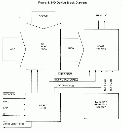
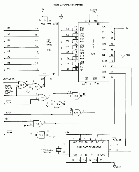
Figure 3. UART Pin Functions
| PIN |
NAME (SYMBOL) |
FUNCTION |
| 1 |
Power Supply (Vcc) |
+5V Supply |
| 2 |
|
Not connected |
| 3 |
Ground (VGI) |
Ground |
| 4 |
Received Date Enable (RDE) |
A logic "0" on the receiver enable line places the received onto the output lines |
| 5-12 |
Received Data Bits (RD8-RD1) |
These are the 8 data output lines. Received characters are right justified: the LSB always appears on RD1. These lines have tristate outputs, i.e., they have the normal TTL output characteristics when RDE is "0" and a high impedance state when RDE is "1" Thus, the data output lines can be bus structure oriented. |
| 13 |
Parity Error (PE) |
This line goes to a logic "1" if the received character parity does not agree with the selected parity. Tri-state. |
| 14 |
Framing Error (FE) |
This line goes to a logic "1" if the received character has no valid stop bit. Tri-state. |
| 15 |
Over-Run (OR) |
This lines goes to a logic "1" if the previously received character is not read (DAV line not reset) before the present character is transferred to the receiver holding register. Tri-state. |
| 16 |
Status Word Enable (SWE) |
A logic "0" on this line places the status word bits (PE, FE, OR, DAV,TBMT) onto the output lines. Tri-state. |
| 17 |
Receiver Clock (RCP) |
This line will contain a clock whose frequency is 16 times (16X) the desired receiver baud |
| 18 |
Reset Data Available (RDAV) |
A logic "0" will reset the DAV line. The DAV F/F is only thing that is reset. |
| 19 |
Data Available (DAV) |
This line goes to a logic "1" when an entire character has been received and transferred to the receiver holding register. Tristate-Fig. 16 |
| 20 |
Serial Input (SI) |
This line accepts the serial bit input stream. A Marking (logic "1 ") to spacing (logic "0") transition is required for initiation of data reception. Fig. 15,16. |
| 21 |
External Reset (XR) |
Resets all registers except the control bits register, Sets SO, EOC and TBMT to a logic "1". Resets DAV and error flags to "0". Clears input data buffer. Must be tied to logic "0" when not in use. |
| 22 |
Transmitter Buffer Empty (TBMT) |
The transmitter buffer empty flag goes to a logic "1" when the data bits holding register may be loaded with another character. Tri-state. See Fig. 9, 11. |
| 23 |
Data Strobe (DS) |
A strobe on this line will enter the data bits into the data bits holding register. Initial data transmission is initiated by the rising edge of DS. Data must be stable during entire strobe. |
| 24 |
End of Character (EOC) |
This line goes to a logic "1" each time a full character is transmitted. It remains at this level until the start of transmission of the next character. See Fig. 8, 10. |
| 25 |
Serial Output (SO) |
This line will serially, by bit, provide the entire transmitted character. It will remain at a logic "1" when no data is being transmitted. |
| 26-33 |
Data Bit Inputs (DB1-DB8) |
There are up to 8 data bit input lines available. |
| 34 |
Control Strobe (CS) |
A logic "1" on this lead will enter the control bits (EPS, NB1, NB2, TSB, NP) into the control bits holding register. This line can be strobed or hard wired to a logic "1" level. See Fig. 19. |
| 35 |
No Parity (NP) |
A logic "1" on this lead will eliminate the parity bit from the transmitted and received character (no PE indication). The stop bit(s) will immediately follow the last data bit. If not used, this lead must be tied to a logic "0". |
| 36 |
Number of Stop Bits (TSB) |
This lead will select the number of stop bits, 1 or 2, to be appended immediately after the parity bit. A logic "0" will insert 1 stop bit and a logic "1" will insert 2 stop bits. The combined selection of 2 stop bits and 5 bits/character will produce 1 1/2 stop bits |
| 37-38 |
Number of Bits/Character (NB2, NB1) |
These two leads will be internally decoded to select either 5, 6, 7 or 8 data bits/character.
NB2 NB1 Bits/Character
0 0 5
0 1 6
1 0 7
1 1 8
|
| 39 |
Odd/Even Parity Select (EPS) |
The logic level on this pin selects the type of parity which will be appended immediately after the data bits. It also determines the parity that will be checked by the receiver. A logic "0" will insert odd parity and a logic "1" will insert even parity. |
| 40 |
Transmitter Clock (TCP)
|
This line will contain a clock whose frequency is 16 times (16X) the desired transmitter baud. |
Figure 4. Baud Rate Generator
PIN FUNCTIONS
| PIN NO. |
SIGNAL |
DESCRIPTION |
| 1 |
XTAL/EXT1 |
Input is either one pin of the crystal package or one polarity of the external input. |
| 2 |
Vcc |
Positive power supply-normally +5V |
| 3 |
fR |
This output runs at a frequency selected by the Receiver divisor select data bits. |
| 4-7 |
RA, RB, RC, RD |
These inputs, as shown in Table 1, select the receiver output frequency, fR. |
| 8 |
STR |
A high level input strobe loads the receiver data (RA, RB, RC, RD) into the receiver divisor select register. This input may be strobed or hard-wired to a high level. |
| 9 |
NC |
|
| 10 |
NC |
|
| 11 |
GND |
Ground |
| 12 |
STT |
A high level input strobe loads the transmitter data (TA, TB, TC, TD) into the transmitter divisor select register. This input may be strobed or hard-wired to a high level. |
| 13-16 |
TD, TC, TB, TA |
These inputs, as shown in Table 1, select the transmitter output frequency ft |
| 17 |
ft |
This output runs at a frequency selected by the Transmitter divisor select data bits. |
| 18 |
XTAL/EXT2 |
This input is either the other pin of the crystal package or the other polarity of the external input. |
REFERENCE FREQUENCY 4.915200MHz
Divisor
Select
DCBA |
Desired
Baud
Rate |
Clock
Factor |
Desired
Frequency
(KHz) |
Divisor |
Actual
Baud
Rate |
Actual
Frequency
(KHz) |
Deviation |
| 0000 |
50.00 |
16X |
0.80000 |
6144 |
50.00 |
0.800000 |
0.0000% |
| 0001 |
75.00 |
16X |
1.20000 |
4096 |
75.00 |
1.200000 |
0.0000% |
| 0010 |
110.00 |
16X |
1.76000 |
2793 |
109.93 |
1.758983 |
0.0100% |
| 0011 |
134.50 |
16X |
2.15200 |
2284 |
134.50 |
2.152000 |
0.0000% |
| 0100 |
150.00 |
16X |
2.40000 |
2048 |
150.00 |
2.400000 |
0.0000% |
| 0101 |
300.00 |
16X |
4.80000 |
1024 |
300.00 |
4.800000 |
0.0000% |
| 0110 |
600.00 |
16X |
9.60000 |
512 |
600.00 |
9.600000 |
0.0000% |
| 0111 |
1200.00 |
16X |
19.20000 |
256 |
1200.00 |
19.200000 |
0.0000% |
| 1000 |
1800.00 |
16X |
28.80000 |
171 |
1796.49 |
28.743859 |
0.1949% |
| 1001 |
2000.00 |
16X |
32.00000 |
154 |
1994.81 |
31.916883 |
0.2697% |
| 1010 |
2400.00 |
16X |
38.40000 |
128 |
2400.00 |
32.000000 |
0.0000% |
| 1011 |
3600.00 |
16X |
57.60000 |
85 |
3614.11 |
57.825882 |
0.3921% |
| 1100 |
4800.00 |
16X |
76.80000 |
64 |
4800.00 |
76.800000 |
0.0000% |
| 1101 |
7200.00 |
16X |
115.20000 |
43 |
7144.19 |
114.306976 |
0.7751% |
| 1110 |
9600.00 |
16X |
153.60000 |
32 |
9600.00 |
153.600000 |
0.0000% |
| 1111 |
19200.00 |
16X |
307.20000 |
16 |
19200.00 |
307,200000 |
0.0000% |
REFERENCE FREQUENCY=5.068800MHz
Divisor
Select
DCBA |
Desired
Baud
Rate |
Clock
Factor |
Desired
Frequency
(KHz) |
Divisor |
Actual
Baud
Rate |
Actual
Frequency
(KHz) |
Deviation |
| 0000 |
50.00 |
16X |
0.80000 |
6336 |
50.00 |
0.800000 |
0.0000% |
| 0001 |
75.00 |
16X |
1.20000 |
4224 |
75.00 |
1.200000 |
0.0000% |
| 0010 |
110.00 |
16X |
1.76000 |
2880 |
110.00 |
1.760000 |
0.0000% |
| 0011 |
134.50 |
16X |
2.15200 |
2355 |
134.52 |
2.152357 |
0.0166% |
| 0100 |
150.00 |
16X |
2.40000 |
2112 |
150.00 |
2.400000 |
0.0000% |
| 0101 |
300.00 |
16X |
4.80000 |
1056 |
300.00 |
4.800000 |
0.0000% |
| 0110 |
600.00 |
16X |
9.60000 |
528 |
600.00 |
9.600000 |
0.0000% |
| 0111 |
1200.00 |
16X |
19.20000 |
264 |
1200.00 |
19.200000 |
0.0000% |
| 1000 |
1800.00 |
16X |
28.80000 |
176 |
1800.00 |
28.800000 |
0.0000% |
| 1001 |
2000.00 |
16X |
32.00000 |
158 |
2005.06 |
32.081013 |
0.2532% |
| 1010 |
2400.00 |
16X |
38.40000 |
132 |
2400.00 |
38.400000 |
0.0000% |
| 1011 |
3600.00 |
16X |
57.60000 |
88 |
3600.00 |
57.600000 |
0.0000% |
| 1100 |
4800.00 |
16X |
76.80000 |
66 |
4800.00 |
76.800000 |
0.0000% |
| 1101 |
7200.00 |
16X |
115.20000 |
44 |
7200.00 |
115.200000 |
0.0000% |
| 1110 |
9600.00 |
16X |
153.60000 |
33 |
9600.00 |
153.600000 |
0.0000% |
| 1111 |
19200.00 |
16X |
307.20000 |
16 |
19800.00 |
316.800000 |
3.1250% |
_______________________________________________________________________________
4
The Toolbox
PARALLEL BUS REVEALED
Conclusion of the first-ever PBI usage guide by EARL RICE
Concluding the four-part series that for the first time teaches advanced XL users how to build an I/O connector for the powerful, ultra-fast Parallel Bus Interface. This article includes an assembly language listing that requires MAC/65 or Atari Assembler Editor. You will also need access to an EPROM burner. The three earlier installments ran in the January, February and March 1985 issues of Antic.
Last month we looked at a design for a serial I/O device using a readily available USART chip. This month we'll design address decoding logic for the device and see how to add a status register and an interrupt register to it. We'll also look at some example software for the device ROM. But first, a little about last month's design.
This USART design is a simplest case design. Writing to any address in the $D100-$D1FF range puts a character into the transmit buffer and it will be sent out the serial I/O line. Reading any address in the same range gets the last received character from the receive buffer.
The easiest way to test this arrangement is to tie the serial input and output lines (USART pins 20 and 25) together. If you write a character to the transmit buffer and wait a few milliseconds, you should be able to read the same character from the receive buffer. All this assumes that we're decoding addresses and that we have some software in ROM, so let's get on with those details.
ADDRESS DECODER
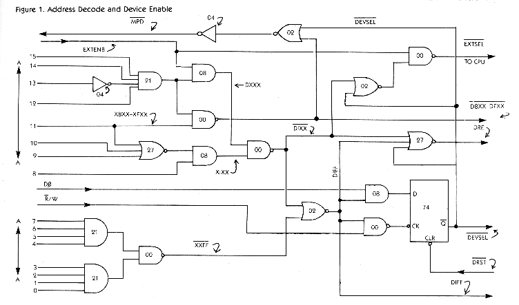
Figure 1 is a schematic diagram of an address decoder to provide ROM selection and device register selection.
The output signal $D8XX-$DFXX, combined with the Device Select signal (DEVSEL), provides the Math Pack Disable signal (MPD) to disable the floating point ROM in the CPU so it doesn't contend with our ROM for the data bus. We can use the same signal to select our ROM. This allows us to remove some of the logic from last month's circuit. Just remove the wires from 1C4 pins 6, 5, 4,13,12 and 11 and connect MPD to ROM pin 20. (See last month's Figure 2).
The signal $DlFF selects the Device Enable Latch. When a write signal clocks the 74HCT74 latch, the value of the Data 0 line (D0) will be stored. Writing 1 to address $DlFF selects our external device. Writing 0 deselects it. $DlFF can also be used later to select an interrupt register.
By combining it with DEVSEL and $DlXX, we get a Device Register Enable signal (DRE). We'll use this signal instead of part of the logic in last month's circuit to make the device registers work. Just remove the wires from 1C4 pins 3,2 and 1, and connect DRST to 1C5 pin 13.
The CPU External Enable signal (EXTENB) lets our device know the computer wants to talk to device registers (or RAM in a more complex application). That signal is combined with DEVSEL and $DlXX to make an External Select signal (EXTSEL) to turn off CPU RAM so as to avoid bus contention.
DEVICE RESET
The Device Reset signal (DRST) comes from last month's circuit and resets the device select latch any time the CPU generates a RESET signal.
You've probably noticed that this month's schematics are a little different from last month's. Since last month's circuit is the basic recipe for our device, we included IC location assignments and pin numbers.
This month's article deals with several options you might or might not use, so we're giving you IC type numbers and no pin assignments for general logic functions. The number inside or next to a symbol is its type number. For example, 00 means 74HCT00.
Since all the logic is 74HCT series, we just need to use the last digits of the type number to identify a part. Also, be aware that we use both positive and negative names for some signals. R/W and R/W are complementary signals and mixing them up won't work.
It would be nice to have a status register. That way, we could tell the state of our USART by asking it, rather than just hoping the byte we gave it got sent, or assuming the byte we got from it is a good one. The USART does have a status word available: four bits to read and a reset bit to write to.
The read bits are three error bits: Over-Run (OR), Framing Error (FE) and Parity Error (PE), and a Transmit Buffer Empty bit (TBE). The write bit is a Reset Data Available bit (RDAV). Last month's signal name list explains these bits's functions.
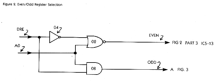
In order to use this new register, we need to expand our addressing capability. Figure 2 shows a way to use the Address 0 line to select even and odd addresses in the device register space.
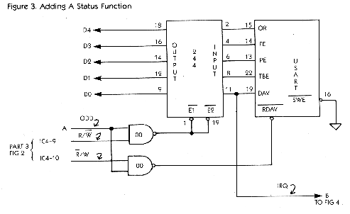
STATUS REGISTER
Figure 3 shows an implementation of the status register. The 74HCT244 shown is a tri-state buffer. This allows us to read the status bits when we select any odd address in the device register space. The gate to the USART RDAV pin resets the Data Available flip-flop when we write anything to an odd address.
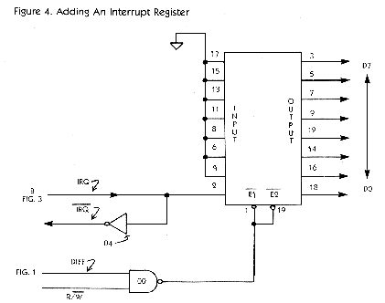
The IRQ line is there in case you want to design in an Interrupt Register. We're assuming that we want to generate an interrupt when we get a Data Available signal from the USART.
Figure 4 uses a 74HCT244 to make an interrupt register. This allows the OS interrupt handler to poll our Parallel Bus device to see who made an interrupt request. By putting the IRQ signal on the Data 0 line, we have established our USART device as Device 0.
Putting the signal on the Data 1 line would make it Device 1, Data 3 makes it Device 3, etc. Whatever bit you use here must correspond to the bit you use for the Enable Latch (Figure 1). The remaining bits must be tied to 0 (Ground).
Remember that we've designed this circuit to be the only external device on the parallel bus. If you were to put several devices on the bus, things would get much more complex. Designing a multiple board system is beyond the scope of this article.
But if you're a serious hardware hacker, you can probably extend what we've done here for more than one function. You should also realize that the logic in this design can be streamlined in several places. We aimed for use of only a few IC types, and haven't always optimized for speed or elegance. Sometimes we do things like use a NOR and an inverter to make an OR gate. Bulky, but workable.
YOUR SOFTWARE
Now for software The only really awkward thing here is that you've got to have access to an EPROM programmer for 2716's. I used a cranky home-built programmer a friend put together. Most large users' groups have at least one member with access to one, so you might try there. The important part of the ROM is the vector table. You can put all your device driver routines on disk and load them as an AUTORUN.SYS file if you want, but the vector table MUST be in ROM. You can also put your device drivers in ROM if you want.
For our example, we are only implementing INIT, PUT, GET, and STATUS. For simplicity, we're making the drivers contiguous with the ROM vector table to run entirely from ROM.
The drivers in Listing 1 were written using MAC/65 (Optimized Systems Software). The source code will also assemble using the Atari Assembler Editor cartridge.
The drivers are thoroughly commented so it should be easy for you to see how they work. Notice that we reset the CRITIC flag at the beginning of each driver routine. The Generic Handler sets it in advance in case a parallel device is extremely time critical.
Forgetting to reset CRITIC defeats some OS functions such as software counter timers and key repeat among others. The rest of the code is very straightforward. Many thanks to Dave Menconi, formerly of Atari, for the easy-to-follow listing.
Using these basic ideas with some ingenuity, you should be able to design your own parallel devices for your 800XL or 600XL computer. If you dream up an interesting project, the editors at Antic would like to hear about it.
Earl Rice headed users' group support and was an engineering project leader for Atari.
Download:

PBI.M65 (2,49 kb)
____________________________________________________________________________________

Vaše hodnotenie, Rate post: