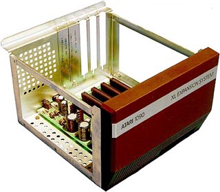
Atari 1090 XL Expansion System - zariadenie na rozšírenie našich ATARI. Bohužiaľ skončilo to na prototypoch a vo vývoji sa nepokračovalo. Veľká premárnená príležitosť.
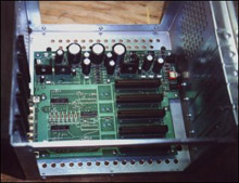
Každé zariadenie má v sebe dva sériové RS-232C a paralelný Centronics, okrem toho, že je vybavené piatimi slotmi pre rozširujúce karty. (Pôvodne sa počítalo až s 8 slotmi.)
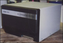
Pôvodne mali byť k dispozícii nasledovné karty:
- Disk Drive Controller
- Votrax Syntezator
- Modem (300 and/or 1200)
- Touch Tone Decoder
- EPROM Programmer
- BSR Controller Interface
- Relay Switch Card
- IEEE 488 Control Card
- Real Time Clock
- 80 Column Display
- Printer Spooler/Buffer
- APPLE Card
- VCS Adapter Card
- A/D Converter Card
- Infra Red Interface
- Hard Disk Interface
- Music Card
- Speech Recognition
- Ram Disk
- Battery Back-up CMOS RAM
- Corvus Interface
- Ethernet Interface
- RAM expansion
- CP/M card
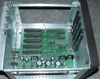
Iba niektoré z týchto kariet dosiahli fázu prototypu, ale aj tak nikdy nevstúpili do výroby. Predpokladá sa, že jednotiek ATARI 1090 sa vyrobilo asi 50 kusov, kompletných jednotiek (s horným krytom) je na svete asi 5 kusov.
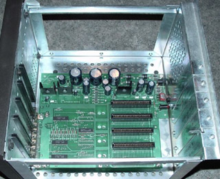
Rozhranie prišlo na svet v nevhodnej dobe, práve sa zmenil majiteľ (nastúpil Jack Tramiel) a rozhodnutie o utlmení výroby pre 8bity sa osudovo podpísalo na tejto vecičke (a nielen na nej ...). Večná škoda, rozvoj týmto smerom mohol byť obrovský, ale dejiny sa píšu aj zlými rozhodnutiami. Predstava bezproblémového chodu CP/M, DOSu by bola udržala ATARI pri živote omnoho dlhšie.
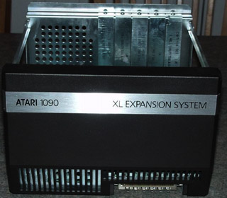
Karty mohli byť nadradené nad počítačom, t.j mohli tu byť založené karty s výkonnejšími procesormi, ktoré by potom "ovládali" ATARI. Počítalo sa s procesormi napríklad: 6518, 8086.
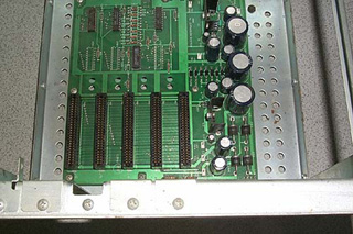
Nasleduje pár kariet, aj keď nie sú úplné a pravdepodobne nikdy neboli plne otestované:
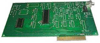
CP/M card
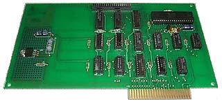
80 Column - bez tejto karty by CP/M ťažko fungovalo
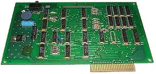
64 KB modul RAM, v 1090-ke mohli byť až 3 tieto moduly
(=192kB RAM)
Neúplný popis špecifikácie je tu:

ATARI 1090XL
_____________________________________________________
17.11.2010
- zohnal som ešte niečo:
1090XL 80-column. OS - OS pre prototyp videokarty
1090XL 80-column. char.set - znaková sade pre videokartu
Obidva OS sú určené na napálenie do Eprom 2716

1090XL 80column.OS
_________________________________________________________________________________
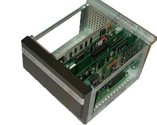
18.11.2010 - ešte jedna fotografia, osadená celá 1090-ka, 5 dosák, bohužiaľ nepríliš vidno čo tam je osadené
_________________________________________________________________________________
14.05.2016
Technická špecifikácia PBI:
PARALLEL BUS INTERFACE Specifications Ajay Chopra Draft of 2/3/83 ATARI COMPANY CONFIDENTIAL
1.0 THE PARALLEL BUS INTERFACE (PBI)
The Parallel Bus Interface Connector is a 50-pin connector (See figure 1.0) with the following signals:
PIN 3 through PIN 9 are AO through A6 respectively. PIN 11 through PIN 18 are A7 through A14 respectively. PIN 20 is A15. These are the CPU address lines. The CPU addresses the Parallel Bus Interface devices using these lines.
PIN 21 through PIN 28 are DO through D7 respectively. These are the processor data lines. The CPU transmits and receives data and control information from the Parallel Bus Interface devices on these lines.
PIN 31 is for the Buffered Phase 2 Clock (BO2) Output to the
Parallel Bus Interface devices.
PIN 35 is the IRQ (Interrupt Request) input from the Parallel Bus Interface devices. A PBI device can pull this input low to invoke the device handler that services the parallel bus device. This input is "open drain".
PIN 46 is the Latched Read/Write (LR/W) Output to the Parallel
Bus Interface devices. This line is "high" for a read cycle.
It is "low" for a write cycle.
PIN 34 is the Reset (POR) output to the Parallel Bus Interface devices. This output resets any device so designed on-power up and when the RESET key on the CPU keyboard is hit.
PIN 49 is audio in signal from the Parallel Bus devices. This line is connected directly to the audio summation network of the CPU. The audio signal is 1 volt Peak to Peak.
CONSOLE
TOP
_________
GND |1 2 | EXT SEL
| |
AO |3 4 | A1
| |
A2 |5 6 | A3
| |
A4 |7 8 | A5
| |
A6 |9 10| GND
| |
A7 |11 12| A8
| |
A9 |13 14| A10
| |
All |15 16| A12
| |
A13 |17 18| A14
| |
GND |19 20| A15
| |
DO |21 22| D1
| |
D2 |23 24| D3
| |
D4 |25 26| D5
| |
D6 |27 28| D7
| |
GND |29 30| GND
| |
B02 |31 32| GND
| |
Reserved |33 34| RST
| |
IRQ |35 36| RDY
| |
Reserved |37 38| EXTENB
| |
Reserved |39 40| REF
| |
CAS |41 42| GND
| |
TD |43 44| RAS
| |
GND |45 46| LR/W
| |
Reserved |47 48| Reserved
| |
AUDIO |49 50 | GND
__________
FIGURE 1.0 PBI CONNECTOR
(Looking into the CPU Connector)
CONSOLE
BOTTOM
PIN 38 is External Decoder Enable (EXTENB) output. This output goes high
when an address on the CPU bus is an allowed address for a PBI device.
The CPU generates the EXTENB signal for all segments of the CPU memory map except:
(a) The Active segments of the O.S. ROM. Any disabled segments
of the O.S. ROM generate the EXTENB signal when addressed.
(b) The region occupied by the internal cartridge (if present).
PIN 2 is the External Select (EXTSEL) Input. This input is generated
by the (external) decoder resident in the PBI device. This signal should
go low whenever the EXTENB is enabled and the selected PBI device
uses the address generated on the CPU Bus. This input is used to disable
the CPU decoder for the duration of the current bus cycle.
PIN 36 is the RDY input to the CPU. A slow PBI device can extend
the CPU bus cycle by pulling this line low when it is addressed.
PIN 40 ' is the Refresh (REF) output. This output may be used for the
refresh timing of volitile memories connected to the PBI.
PIN 43 is Math Pak Disable (MPD) input from the PBI devices.
This input is pulled to the "low" state whenever a Parallel Bus device is
selected by the CPU and the device has a handler resident in the region D800H to DFFFH.
PIN 44 is ROW Address Strobe (RAS) output to the Parallel Bus devices.
This output may be used for external memory expansion.
PIN 41 is the Column Address Strobe (CAS) output to the Parallel Bus
devices. This output may be used for external memory expansion.
PINS 33, 37, 39, 47 and 48 are reserved.
PINS 1, 10, 19, 29, 30, 32, 42, 45 and 50 are Signal grounds (GND).
ELECTRICAL LEVELS:
D. C. Characteristics
All PBI outputs from the CPU will have tne capability of driving one
LSTTL gate.
All PBI inputs except IRQ should have the drive capability of the
output of an LSTTL gate.
The 1RQ input is "open drain" and in the "low" state should present
the following characteristics:
11 = 0.4V (max) I = 1.6mA (min Sink current)
AC Characteristics
To be specified.
2.0 Parallel Bus Devices
The Parallel bus will support three types of devices:
2.1 External Memory:
The PBI will allow the user to expand the local RAM externally to
- up to 64K. This will allow external memory expansion of a 16K CPU.
2.2 Parallel Bus Peripherals (PBPS)
The PBPs have the following characteristics:
(a) They interface to the CPU through a well defined handler/O.S. interface. The code for this interface is resident in CPU Memory location D600H to D7FFH (COMM A & COMM B areas). The ROM containing this code is physically located in a Parallel Bus Adapter. (See Section 3.0)
The O.S. can support up to 8 PBPs at one time.
(b) Each PBP has a unique handler that resides in-the CPU memory space at locations D800H to DFFFH. The ROMs containing the code for these handlers are physically resident in the respective peripherals. (The memory space occupied by the handlers actually contains the @lath-pak within the S-16. The Math-pak is disabled whenever any EBP is enabled. See (c) below).
(c) Location DIFFH in the CPU memory map is reserved for passing control information between the CPU and the PBPS.
The CPU linearly selects the PBI devices by writing into location DLFFH.
Location DLFFH.
Writing a "1" into Dx (x=O to 7) selects device Dx (x=O to 7).
Writing a "O" into Dx (x=O to 7) de-selects device Dx (x=O to 7).
The CPU can thus select up to 8 PBI devices.
If the IRQ line is pulled "low" the CPU polls location DLFFH.
A read from this location returns the PBI devices' interrupt
status.
2. 2 Parallel Bus Peripherals (PBPS) (continued)
(c) continued....
if bit Ix (x=O to 7) is "1", then device Dx (x=O to 7) has interrupted. If bit Ix (x=O to 7) is "O" then device Dx (x=O to 7) has not interrupted. The device is required to clear its interrupt status bit when its interrupt is ser-viced by the CPU.
2.3
(d) The PBPs should assert MPD only when they are selected. The PBPs should assert EXTSEL only when they are selected and if EXTENB is asserted.
(e) The PBPs may respond to any one of the selects Dl through D7. It is recommended that the PBPs have configuration switches to allow them to respond to any one of the selects Dl through
D7. The PBPs should not respond to device select DO. DO is
reserved for use by Atari.
(f) A peripheral handler may respond to address in the region D80OH-DFFH only when it is selected. Location D800H contains the device I.D. of an PBP. If a slot that contains no peripheral is selected, address D800H should return FFH as data.
(g) A peripheral may respond to addresses in the region DIOOH to DLFEH only wben it is selected.
(h) The PBPs will have priority over the SIO peripheral when they are addressed generically.
(i) The data between the CPU and an PBP is passed under the control of the peripheral handler for the PBPS.
(j) The PBPs will work if a cartridge is present in the cartridge slot.
"External Application" Cartridges:
The External Application Cartridge are a generalization of the PBPS.
They have the following characteristics:
(a) An "External Applications" Cartridge (EAC) can reside at any or all of the addresses in the region OOOOH to BFFFH for which the EXTENB is generated. They may respond to these addresses only when "opened."
(b) The EACs must be "opened" by the S-16 through the slot select location in the same was as the PBPS.
(c) The EACs must conform to the EXTENB/EXTSEL protocol.
2. 3 "External Application" Cartridges: (continued)
(d) The EACs must have a "handler" (resident in locations D800H to DFFFH) that controls their operation. The EACs must conform to conditions (d) thru (g) of Section 2.2 above.
(e) The EACs will work if a cartridge is present in the internal cartridge slot.
3.0 THE PBI ADAPTER CONCEPT:
The use of the PBI shall require a PBI adapter. The PBI adapter shall provide, at a minimum, the following:
(1) Buffers for the Address, Data, LR/W, B02, RAS, CAS, RST, REF and EXTENB Signals.
(2) 512 bytes of ROM that contain code for the CPU's software interface to the PBPS. This code is resident in locations D600 to D7FF in the CPU memory map. The Adapter will have to decode this address space to generate Chip Select for the ROM.
Any PBI device that does not use the PBI adapter will have to provide (1) above. It will also have to provide (2) above if it is a PBP or an EAC.
The PBI adapter may optionally provide the following in addition to (1) and (2) above:
(a) The memory expansion for a CPU that has less than 64K RAM.
(b) Device Select address decode (DIFFH and write). This decode may be bussed to the PBI devices connected after the adapter on one of the reserved lines.
(c) IRQ Status decode (DIFF and read). This decode may be bussed to the PBI devices connected after the adapter on-one of the reserved lines.
(d) Power Supply to support the PBI devices connected to the adapter. Such a power supply may source +5, +12 and -12V. These power signals may be bussed to devices connected after the adapter on reserved lines.
____________________________________________________________

Vaše hodnotenie, Rate post: